- 您现在的位置:买卖IC网 > Sheet目录1994 > DS3105LN+ (Maxim Integrated Products)IC TIMING LINE CARD 64-LQFP
DS3105
107
9.3
JTAG Instruction Register and Instructions
The instruction register contains a shift register as well as a latched parallel output and is 3 bits in length. When the
TAP controller enters the Shift-IR state, the instruction shift register is connected between JTDI and JTDO. While in
the Shift-IR state, a rising edge on JTCLK with JTMS low shifts data one stage toward the serial output at JTDO. A
rising edge on JTCLK in the Exit1-IR state or the Exit2-IR state with JTMS high moves the controller to the Update-
IR state. The falling edge of that same JTCLK latches the data in the instruction shift register to the instruction
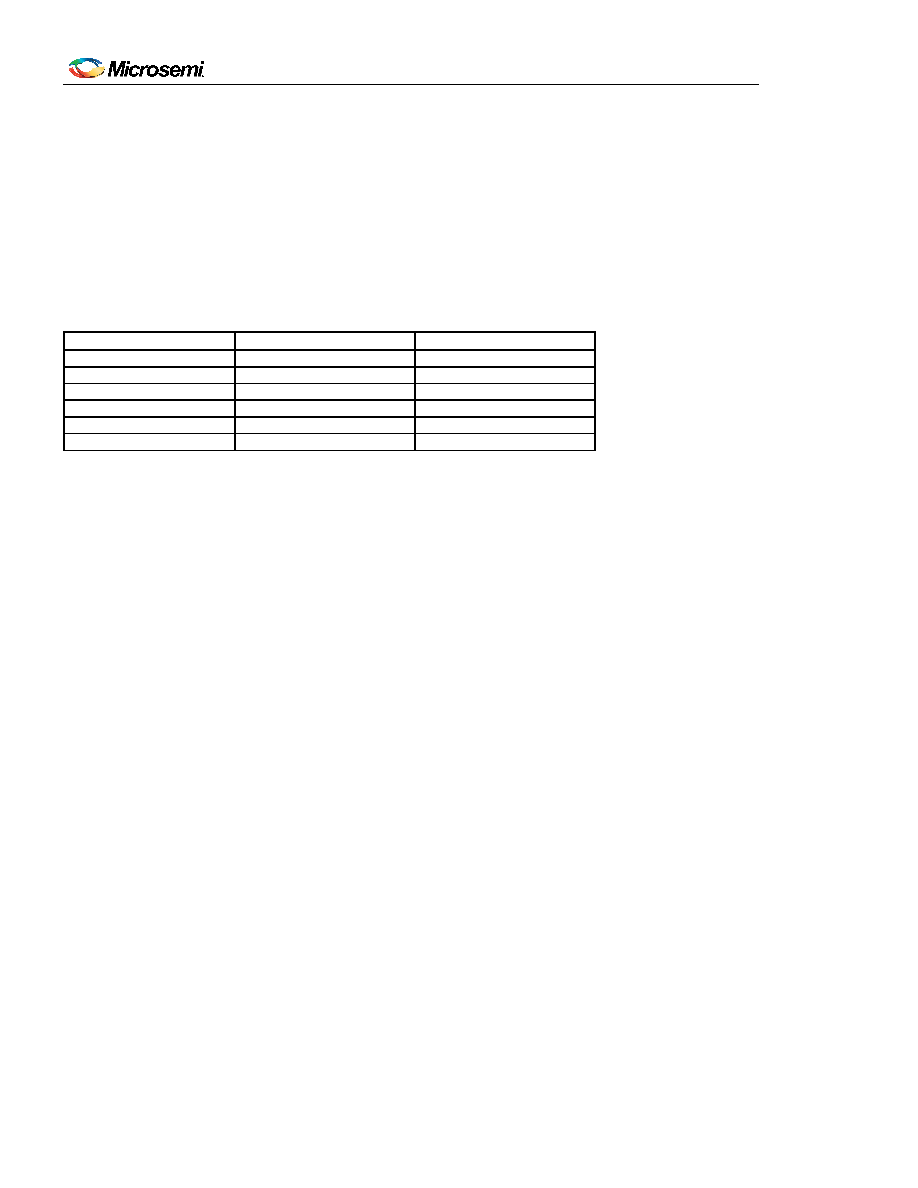
parallel output. Table 9-1 shows the instructions supported by the DS3105 and their respective operational binary
codes.
Table 9-1. JTAG Instruction Codes
INSTRUCTIONS
SELECTED REGISTER
INSTRUCTION CODES
SAMPLE/PRELOAD
Boundary Scan
010
BYPASS
Bypass
111
EXTEST
Boundary Scan
000
CLAMP
Bypass
011
HIGHZ
Bypass
100
IDCODE
Device Identification
001
SAMPLE/PRELOAD. SAMPLE/RELOAD is a mandatory instruction for the IEEE 1149.1 specification. This
instruction supports two functions. First, the digital I/Os of the device can be sampled at the boundary scan
register, using the Capture-DR state, without interfering with the device’s normal operation. Second, data can be
shifted into the boundary scan register through JTDI using the Shift-DR state.
EXTEST. EXTEST allows testing of the interconnections to the device. When the EXTEST instruction is latched in
the instruction register, the following actions occur: (1) Once the EXTEST instruction is enabled through the
Update-IR state, the parallel outputs of the digital output pins are driven. (2) The boundary scan register is
connected between JTDI and JTDO. (3) The Capture-DR state samples all digital inputs into the boundary scan
register.
BYPASS. When the BYPASS instruction is latched into the parallel instruction register, JTDI is connected to JTDO
through the 1-bit bypass register. This allows data to pass from JTDI to JTDO without affecting the device’s normal
operation.
IDCODE. When the IDCODE instruction is latched into the parallel instruction register, the device identification
register is selected. The device ID code is loaded into the device identification register on the rising edge of JTCLK,
following entry into the Capture-DR state. Shift-DR can be used to shift the ID code out serially through JTDO.
During Test-Logic-Reset, the ID code is forced into the instruction register’s parallel output.
HIGHZ. All digital outputs are placed into a high-impedance state. The bypass register is connected between JTDI
and JTDO.
CLAMP. All digital output pins output data from the boundary scan parallel output while connecting the bypass
register between JTDI and JTDO. The outputs do not change during the CLAMP instruction.
发布紧急采购,3分钟左右您将得到回复。
相关PDF资料
DS3106LN+
IC TIMING LINE CARD 64-LQFP
DS3231MZ+
IC RTC I2C 8SOIC
DS3231SN#T&R
IC RTC W/TCXO 16-SOIC
DS3232MZ+
IC RTC W/SRAM I2C 8SOIC
DS3232SN#T&R
IC RTC W/TCXO 20-SOIC
DS3234S#
IC RTC W/TCXO 20-SOIC
DS32C35-33#T&R
IC RTC ACCURATE I2C 3.3V 20-SOIC
DS3911T+
IC DAC 10BIT I2C QUAD 14TDFN
相关代理商/技术参数
DS3106
制造商:MAXIM 制造商全称:Maxim Integrated Products 功能描述:Line Card Timing IC
DS3106A10SL3S(621)
制造商:Amphenol Corporation 功能描述:
DS3106A14S2S
制造商:Amphenol Corporation 功能描述:
DS3106A14S2S(621)
制造商:Amphenol Corporation 功能描述:
DS3106A14S5P
制造商:Amphenol Corporation 功能描述:
DS3106A14S5P(621)
制造商:Amphenol Corporation 功能描述:
DS3106A14S5S(621)
制造商:Amphenol Corporation 功能描述:
DS3106A14S6P
制造商:Amphenol Corporation 功能描述: